Intel to Quadruple Cutting-Edge Chip Packaging Capacity by 2025
August 23, 2023 — Intel aims to quadruple capacity for its most advanced chip packaging services by 2025, including with a new facility in Malaysia, as America’s biggest chipmaker seeks to regain the global lead in semiconductor manufacturing.
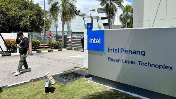
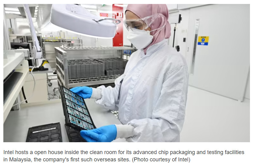
The factory being built in Penang will be Intel’s first overseas facility for advanced 3D chip packaging, what it calls Foveros technology. The company is also building an additional chip assembly and testing factory in Kulim as part of a $7 billion expansion in the Southeast Asian nation.
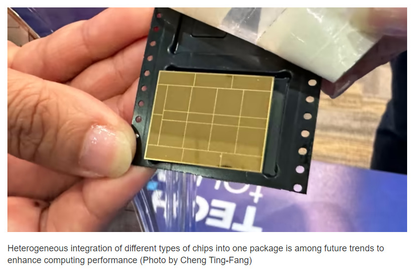
Advanced chip packaging technology combines different types of chips into one package to increase computing power and lower power consumption.
Malaysia will eventually become Intel’s biggest production base for 3D chip packaging, Robin Martin, corporate vice president for manufacturing supply chain and operations, told reporters on Tuesday. The company did not specify when the Penang facility would begin mass production.
Intel said Amazon, Cisco and the U.S. government have committed to using its advanced packaging technology. Intel will also use the tech in its newest central processing unit (CPU) for personal computers, slated to begin shipping this year.
Chip packaging was previously viewed as less crucial and less technologically demanding than chip manufacturing itself. It has emerged as a key area in the race to produce ever more powerful chips as the conventional approach — squeezing more transistors into a smaller area — becomes more difficult.
This year’s generative AI boom has further intensified interest in advanced chip packaging.
Nvidia’s H100, for example, which provides the computing power for the popular ChatGPT chatbot, utilizes Taiwan Semiconductor Manufacturing Co.’s advanced packaging process. This process combines a graphic processor unit (GPU) with six high-bandwidth memory chips to enable high-speed data transmission and the overall performance needed to train large AI language models.
TSMC recently announced plans to build a $2.9 billion facility for advanced chip packaging in Miaoli, Taiwan, to serve growing AI demand.
The market for advanced chip packaging services was worth $44.3 billion in 2022, according to Yole Intelligence, and is expected to grow at a compound annual rate of 10.6% from 2022 to reach $78.6 billion by 2028.
“The latest catalyst for advanced chip packaging is mainly coming from chips handling large models for artificial intelligence,” said Mark Li, a veteran semiconductor analyst with Sanford C. Bernstein.
“Industries are currently eager to invest in AI computing and the capacity of advanced packaging is being expanded to address that. Nonetheless at the end of the day, AI applications still need to proliferate to justify the enthusiasm being sustained in the future.”
Intel’s 3D chip packaging technology is currently developed primarily in the U.S. state of Oregon and its major production base is in the state of New Mexico. The company plans to spend a total of more than $10 billion on this area in New Mexico and Malaysia over the next decade.
Intel said it is speaking with multiple customers and is willing to offer chip packaging services even if customers do not produce chips with Intel’s foundry service.
Intel previously focused on manufacturing, packaging, assembling and testing its own chips internally. It has undertaken a massive transformation in recent years to open up these services to external clients to create new growth drivers.
Steve Long, Intel’s corporate vice president of sales and marketing for Asia Pacific and Japan, said the company’s global production footprint will help attract customers for manufacturing and packaging services. “There is one company today that has the breath of resiliency and breadth of global presence already,” Long said. “That is Intel.”
Malaysia is already a vital chip packaging, assembly and testing base for Intel, which employs 15,000 staff in the country, including 6,000 at its chip design center.
In India, Intel operates its biggest design and engineering center outside of the U.S. with 14,000 employees.
Intel also operates advanced chip manufacturing sites in Ireland and Israel and is expanding chip production in Germany and chip packaging facilities in Poland and Vietnam.
Source: Nikkei Asia